
Quality Manufacturing
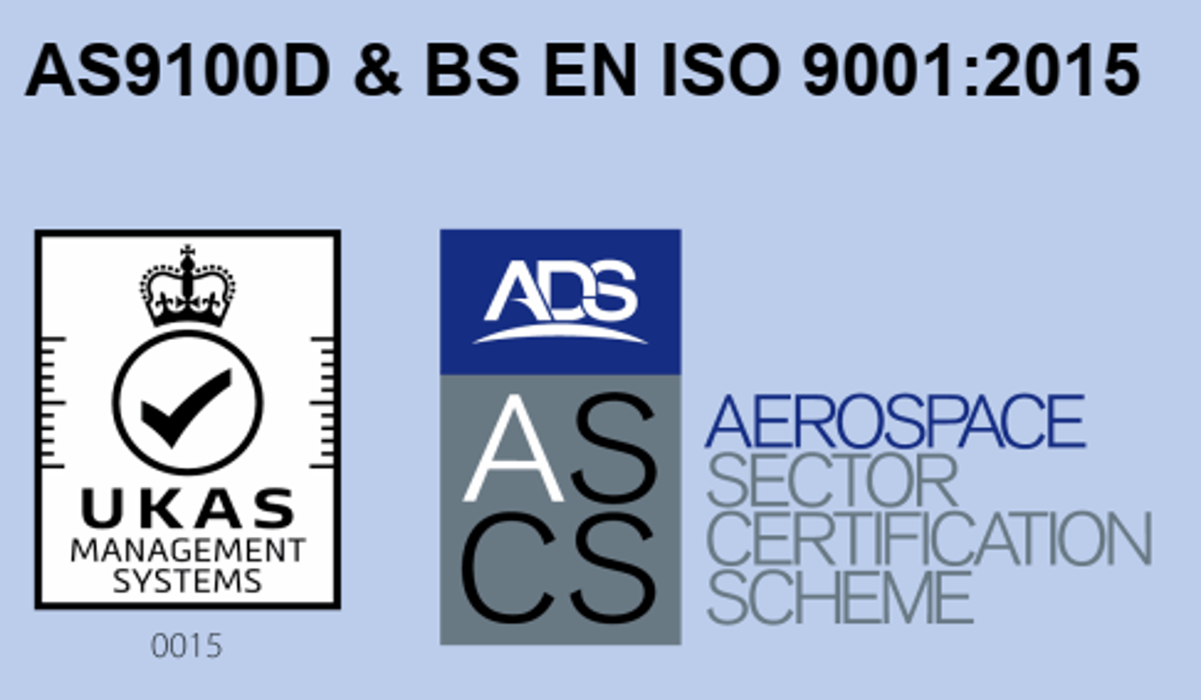
Approval to: AS9100 Rev D - BS EN ISO 9001:2015
High quality product manufacturing is at the heart of the Euroquartz operation. As an independent manufacturer, we value and maintain AS 9100 approval. AS 9100 is an international quality management standard written by the aerospace industry to maintain and improve product quality and assure the integrity of supplies to the industry.
It has been published in Europe as EN 9100, in the United States as AS9100 and in the Far East as SJAC 9100. This standard incorporates all of ISO 9001 with additional industry specific requirements for aerospace. More stringent than ISO9001, this standard is essential for all our military and aerospace customers and in addition, offers all other customers a higher degree of confidence in the quality of the products we produce and supply.
Authorised UK Distributor Agreements
In order to provide our world-wide customer base with a wide range of frequency control product Euroquartz is the authorised distributor for three quartz crystal and oscillator design and manufacturing companies all of which have unique and complementary product ranges. Statek Inc, USA-based, produce a broad line of leading edge, ultra-miniature quartz frequency control devices, providing advanced technical solutions, excellent customer service with superior product quality.
Greenray Industries, USA based, is a leading manufacturer of OCXOs, TCXOs, and VCXOs, precision quartz crystal oscillators that function as precision signal sources for communications, instrumentation and military applications.